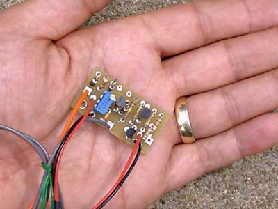
I guess it's ready.
The circuit design was intended for the smaller systems.
It is expected to fill the obvious gap between NO controller and a complicated or expensive controller.
The major design parameters were proper function, versatility, simplicity, ease in understanding, trouble shooting, and obtaining parts. And low cost.
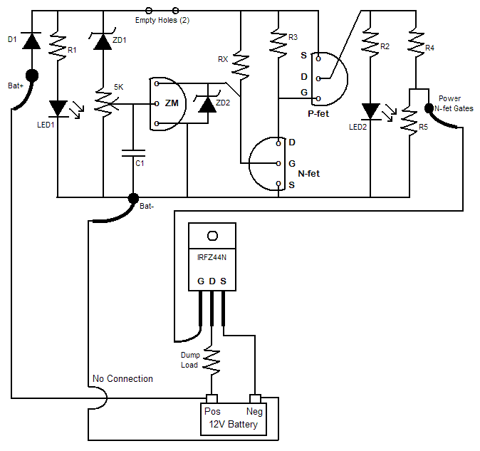
The schematic is a virtual map of the circuit board. Those who prefer a more standard format probably don't need this circuit.
Simple. The PCB was laid out to minimize risk of solder bridges. Nothing has more than 3 legs. Everything except the voltage divider output is On or Off.
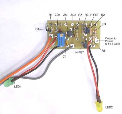
Some mosfets will have a different pin configuration. Be sure to get the G, S, and D in the proper holes.
Understanding the circuit, a crash course:
The rectifier diode protects the circuit against reverse polarity.
The Green LED shows the circuit is connected to the battery.
The Yellow LED shows the circuit is dumping excess power through the dump load, or the item connected to the LVD has power.
The first Zener diode and the pot is a voltage divider used to monitor the battery voltage.
The second Zener diode protects the ZM and 2N7000 mosfet from over voltage conditions.
When the voltage from the pot to the `ZM' is lower than 4.6V, the ZM grounds the 2N7000 gate and the remainder of the circuit is off.
When the voltage from the pot to the `ZM' is higher than 4.6V, the ZM is open and the 2N7000 gate has 5.1V. This turns on the rest of the circuit.
The P Channel mosfet sees low voltage at its gate and it turns on. It supplies voltage to the power mosfet gate, turning it on. The dump load is now on.
The capacitor provides enough delay in cycling to ensure the circuit does not go into excessive oscillation.
The extra steps (from N to P to N) provide a fast hard square switching, and allow for the use of numerous and various models of N channel power mosfets.
Meaning the expensive power mosfets need not be logic level or have an ultra low resistance (if the amps being dumped through it are low enough and the heat sink is large enough). Even a lowly IRF530 can be added to supply 2A to another dump load.
Resistor RX determines the hysteresis. The lower the ohms of RX, the tighter the hysteresis.
Some people or systems want a tighter hysteresis, like 0.06V.
Others desire a little more tolerance, like a hysteresis of 0.15V.
Using the circuit as a low voltage disconnect, a hysteresis of 0.6 or 0.8V is good for me.
A brief parts list.
D1 blocking diode=1N4001 to 1N4007, LED1 is green, LED2 is yellow, LED resistors R1 and R2 = 3.3K (between 2K and 10K), C1= 10uF 16V (between 2.2 and 47uF, 10V minimum), ZD1 and ZD2 = 5.1V, R3=51K, R4= 0 to 500 ohms (lower with many power fets or higher for LVD use, centered on 50 to 100 ohms), R5= 3K to 10K (3K with less hysteresis, or 10K with higher hysteresis, even 100K for use with a low power load for an LVD circuit).
N-fet=2N7000 or similar. About anything that can take +-20V at the gate.
P-fet=BSS92, BS250 or similar. About anything that can take +-20V at the gate.
Power N-fet=IRFZ44N or similar. Any power N-fet can be used, provided the current it carries causes less than the watts of heat it can tolerate and dissipate. The IRFZ44N is a personal favorite because it is cheap, has low resistance, causes less heat, and can take reasonable (6A) current without much heat generation.
I like using a separate dump load for each power N-fet. I have never seen a failure using an IRFZ44N supplying a 6A load. I have seen 5 or 6 parallel IRFZ44Ns consistently fail while conducting less than 20A peak.
A higher hysteresis (like 0.08 or 0.1V) will minimize the chances of a power fet failure.
The RX resistor/hysteresis values. 1.8K/1.0V, 3K/0.8V, 3.9K/0.62V, 51K/0.14V, 100K/0.1V, 150K/0.08V, 180K/0.06V, 220K/0.04V.
Values for RX below 1.8K are getting near the danger zone and are not recommended.
Values above 220K are simply not needed and could cause problems.
It is of the utmost importance the wires for the circuit are separate from the wires supplying the dump load. Otherwise the circuit will see the voltage drop from the dump load as a reduction in battery voltage. The wires MUST be separate.
A fly-back or freewheel diode must be included for many dump or LVD loads, or the voltage spike will ruin the power fet. It is not only for this circuit, it seems to be common for many switching circuits.
Calibrating the unit. I suggest calibration without a dump load connected. If the yellow LED is lighted, the dump load should be on.
A variable voltage supply is easiest. They can be easily made from a LM317 or LM780X (7805, 7806, etc).
A friend has no access to a variable voltage supply. He used a running automobile to obtain 14.15V. Simply 100% Genius. The voltage on some cars (mine) can be slightly varied by turning the headlights or A/C on.
Everyone has their own ideas of what is best. My personal preferences would be...
About 0.08V hysteresis for a dump load, for no particular reason except I think it is enough to accept the charge current, drain the surface charge, and not actually drain the battery (much).
About 0.62V for an LVD, because it is usually enough for what I do, without being too fast. It allows for the loaded battery to reach 12.2V (about where hard sulfation can occur) before disconnecting, and 12.82V before reconnecting (to allow for a bit of voltage due to surface charge).
A switch between the circuit and battery will allow for manual equalization.
The unit can be used for a dump regulator, an LVD, a controller for charging a second or third battery, or about any combination of the above.
It will be available as a 150W kit. Waiting for a few more parts to show up.
The kit will include the PCB and parts shown, an assortment of resistors, 2 power N-fets, some heat shrink tubing, LED retainer clips, etc.
The kit will not include the actual dump load, enclosure, switch, wires, etc.
Looks like $12.50. I'll get it up in Classifieds soon.
Anyone using this circuit feel free to jump in with information or pictures!
Open for questions.
G-
