Author Topic: PCB howto (320 Kb of photos)  (Read 7521 times)

0 Members and 1 Guest are viewing this topic.

commanda

  • Hero Member
  • *****
  • Posts: 731
PCB howto (320 Kb of photos)
« on: July 23, 2006, 09:49:25 AM »
Short version,

Layout with Autotrax; print on laser printer to transfer film; laminate onto copper pcb; etch; trim; drill; populate.


Long version with pics.

Autotrax is a Dos program which runs just fine on Windows if you set it to full screen mode.

It is available from

http://www.altium.com/Products/AltiumDesigner/Licensingoptions/AltiumDesignerProtellicense2004/Downl


oads/AltiumFreewareEndUserLicenseAgreement/Autotrax/

Updated video (and printer) drivers are available from

http://www.airborn.com.au/layout/easytrax.html


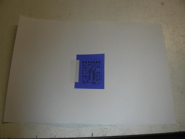
The transfer film I use is called press n peel blue. First I print the copper side image to paper, stick a piece of the blue film over the printout, then feed it through the printer a second time and print onto the blue transfer film.

Make sure you stick it down on the leading edge as it feeds through the printer.

Turn off toner saver and set it to print as dark as possible to impart the maximum amount of toner possible.

This is what it looks like after the second pass through the printer.


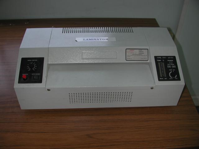
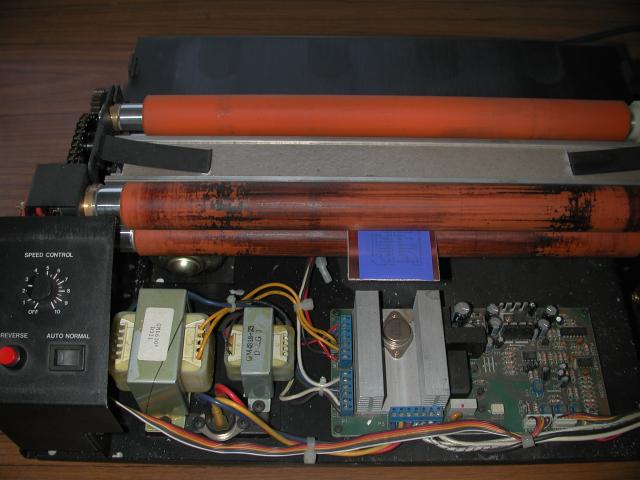
This is the hot laminator I use. Some notes later on a cheaper alternative.

The instructions with the transfer film say to use a hot iron. Take it from me; forget it. You can't get enough heat and pressure using a hot iron.


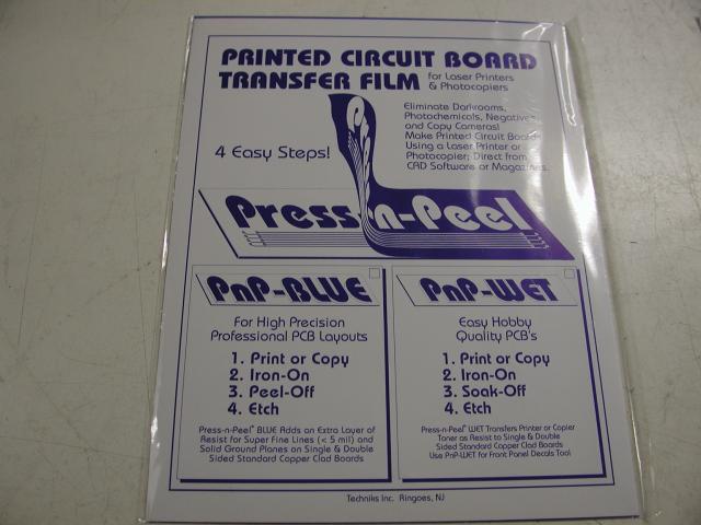
This is the film I use. I source it from Jaycar in Australia, but it should be available world-wide.


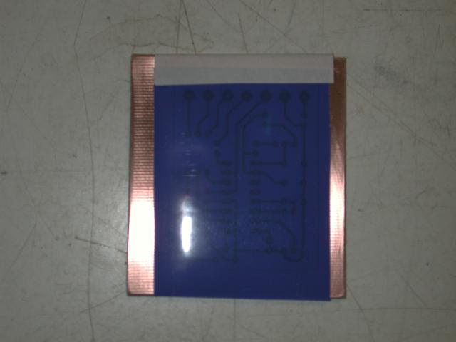
Here's the film set up on a blank piece of copper ready for the laminator. I clean the copper with stainless steel wool, 1200 wet n dry, then finish with isopropanol alcohol. Cleanliness is key at this point. No greasy finger marks.


Feeding the prepared board into the laminator. I remove the cover of the laminator to get easier access to those heated rollers. I set it to 140 deg C and the speed to number 2. Nice and slow and pretty warm. Temperature will vary slightly depending on the toner in your laser printer. Small boards I run through twice. Larger boards I run through 3 times.


After the laminator, drop it straight into cold water and let sit for a few minutes.


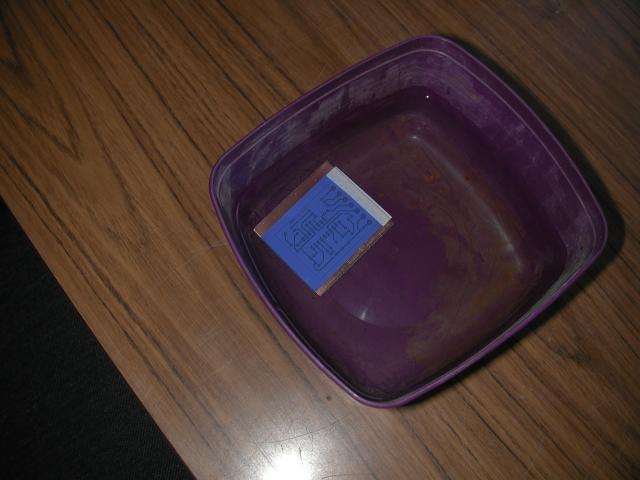
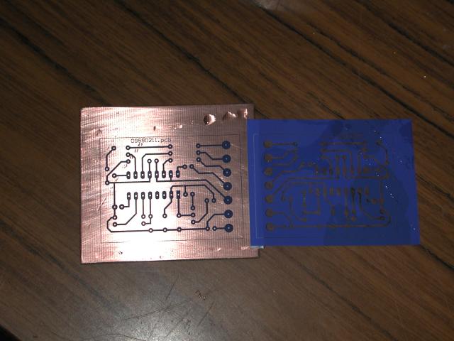
Now the film should just peel away easily, leaving the toner on the pcb.


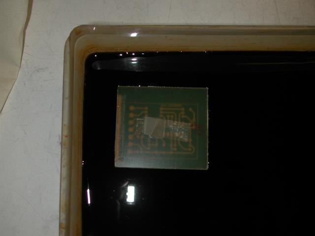
Into the ferric chloride. I float it on top, and make a loop of sticky tape to insert/remove the board.


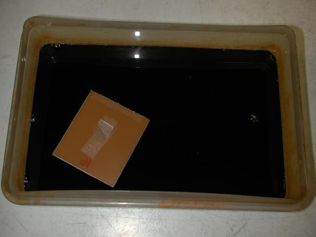
After a few minutes, or longer as the etchant gets used up, it is now etched and ready to be removed and rinsed under cold running water


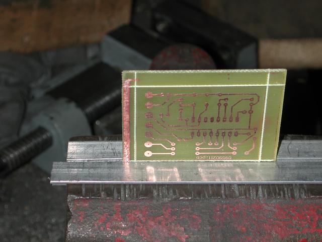
I then score the outline of the pcb with a Stanley knife on both sides (boxcutter in some parts of the world I believe) and snap it in a bench vice.


The sticky paper I use to hold the transfer film in position is manufactured by Avery, and sold as laser printer labels. I use the full A4 size sheets and cut off strips as needed. This stuff will handle the heat of the laser printer and the laminator. Don't try and use sticky tape. This stuff is also great for making meter faces as in my combined metering board.


As for the laminator. I am lucky in that my employer has this laminator that I can use. The rollers are spring loaded, so the thickness of the pcb is not a problem. I did for a while use the heated rollers out of an old HP laser printer until I lost control of the heating elements and cooked it.


You can buy a cheap laminator and modify the rollers to do this. More information on this site;

http://www.pulsar.gs/PCB/a_Pages/4_Products/4d_Toner_Applicator/Toner_Applicator.html

Down near the bottom of the page is a link to a pdf detailing modifications for normal 64 thou pcb.


And there you have it. Less than an hour from an image on the computer to a pcb ready to drill. That time included taking photos and being side-tracked by the boss wanting to work on what he considers real work. That one hour was a lot less than it took me to write this howto.


And if you really want to know, that particular pcb is a switchmode controller pcb for the upcoming Grand Unified Dc-Dc Converter.


Amanda

« Last Edit: July 23, 2006, 09:49:25 AM by (unknown) »

dinges

  • Hero Member
  • *****
  • Posts: 1294
  • Country: nl
Re: PCB howto (320 Kb of photos)
« Reply #1 on: July 23, 2006, 04:51:42 AM »
Interesting. Will check whether I can get the stuff over here (Netherlands) but have serious doubts. Otherwise I'd have remembered it. Farnell perhaps?


BTW, good tip on the scoring of the PCB & breaking/snapping in a vice. Used to saw & file for years. Then I switched to the metal sheet cutter. Works much faster & less wear on the saw blades (glass ruins them quickly). Snapping them off... Will have to remember it.


Grand Unified DC-DC converter (TM). Looking forward to it. Seems an awfully small & simple PCB though for that task. But I'm afraid the GUDCDC (TM) is constructed in 'Amanda modular style' :)

« Last Edit: July 23, 2006, 04:51:42 AM by dinges »
“Research is what I'm doing when I don't know what I'm doing.” (W. von Braun)

Stynus

  • Newbie
  • *
  • Posts: 14
Re: PCB howto (320 Kb of photos)
« Reply #2 on: July 23, 2006, 06:02:45 AM »
Instead of that "press n peel" paper you can use also photopaper for inkjet and then print the layout on it with a laser printer. It's cheaper then the "press n peel".
« Last Edit: July 23, 2006, 06:02:45 AM by Stynus »

JW

  • Development Manager
  • Super Hero Member Plus
  • *****
  • Posts: 4177
  • Country: us
Re: PCB howto (320 Kb of photos)
« Reply #3 on: July 23, 2006, 03:30:12 PM »
Hi Commanda,


 I really enjoy'd reading this post. As somebody who should have learn'd to make PCB's by now, your posting makes me want to try this. Even if I use some different things than you did. I feel I have a good overveiw of the process -thanks.


JW

« Last Edit: July 23, 2006, 03:30:12 PM by JW »

Countryboy

  • Sr. Member
  • ****
  • Posts: 269
Re: PCB howto (320 Kb of photos)
« Reply #4 on: July 23, 2006, 09:11:42 PM »
Hi Amanda,

  Excellent descriptive posting.

  I'm mechanically inclined, so learning how to build a genny comes easy to me, but understanding how to build the electronics side of things is new stuff to me.  I'm in awe of those of you that are gifted with doing this.

  While I don't understand how to design circuits like this, your post gives me a little confidence that I could be a copycat and build a circuitboard like you did, as long as I had the circuit diagram to print out.

Thanks.
« Last Edit: July 23, 2006, 09:11:42 PM by Countryboy »

willib

  • SuperHero Member
  • ******
  • Posts: 2414
  • Country: us
Re: PCB howto (320 Kb of photos)
« Reply #5 on: July 23, 2006, 09:36:53 PM »
I've heard photo paper works real well , and i've had good results with printing the toner on magazine paper , then ironing the toner to the board , and soaking it in water (till all the paper dissolves) but that press n peel stuff looks better , i wonder what its made of ?

« Last Edit: July 23, 2006, 09:36:53 PM by willib »
Carpe Ventum (Seize the Wind)

JW

  • Development Manager
  • Super Hero Member Plus
  • *****
  • Posts: 4177
  • Country: us
Re: PCB howto (320 Kb of photos)
« Reply #6 on: July 26, 2006, 12:08:06 AM »
Hi there CountryBoy,


 If I were you, I wouldn't even mess around with emulation softwhare. I got some, and cant make my damn circuits work like in the demo simulator. But can make them work fine on a breadboard? I just dont know, some believe in electron theory, and some in hole theory. Nevertheless I cant get my grounding points rite :) .


 It 'is' hard to design a circuit from scrach... Guess neccesity 'is' the mother of invention.


JW

« Last Edit: July 26, 2006, 12:08:06 AM by JW »

mrpackethead

  • Newbie
  • *
  • Posts: 10
Re: PCB howto (320 Kb of photos)
« Reply #7 on: November 19, 2006, 01:44:06 PM »
Hi..


I've used the press'n'peel film as well.. Works well, however i've found that i could use the iron as described fine..  Trick was to get it to the right temperture.. I used a K Theromcouple to measure it.. And my results have been fine.. However a friend of mine was having all sorts of trouble.. We put it down to his laser printer and the toner.. He easily made it all work with something printed from my printer.  The laminiator idea is good though, its probably a lot easier if you actually have one.


The price of the press'n'peel certainly put me off ( $25 for 5 sheets ), but i found a alternative source.. the manufacturer sells directly. ( http://www.techniks.com/ ).  They shipped it from the US to New Zealand no problems. I guess that they will ship it anywhere.


The other thing i noted, was that you are using ferric cloride..  Messy stuff, i'm using Ammonium Percholrate, only down side of that is that you need to heat it to about 70deg to get it to work..   However i found that just simply boiling the jug, and then mixing boiling water and the crystals works fine.. I just pour it all into a pyrex baking dish.. ( don't use one from the kitchen, go and buy one, i'm not sure if the chemical is toxic, but for $10, im not keen to find out )

« Last Edit: November 19, 2006, 01:44:06 PM by mrpackethead »